|
|
Fabrication of vertically aligned core-shell nano pillar structure for high sensitive photodetectors
| Abstract: |
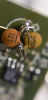
Semiconductor based photodetectors often employ p-i-n junction diodes for detection of photons. Traditional thin film type of structures are made of layers of p type, i type and n type materials. In this type of geometry the photon has to travel through the entire top layer without being absorbed before it reaches the depletion region. This reduces the efficiency of the conversion process. If we can realize an idealized geometry of the p-i-n junction where the photons are directly incident on the depletion region then one can achieve higher quantum efficiencies. Such geometry will also allow us to locally probe in real-time the charge carrier generation, transport and their interactions with defects in the depletion region. In this talk, I will describe clean room fabrication of vertically aligned GaN core-shell nano pillar structure over a large area for high sensitive photo detector applications. I will also describe fabrication of different type p-i-n devices made of Si and SiGe materials. |
| Speaker: |
Dipak Paramanik - Iowa State University |
| Speaker Bio: |
 Dr. Paramanik worked extensively at NanoFab clean room facility at NIST, Gaithersburg in the area of fabrication of semiconductor devices. He also worked at clean room facility at National Institute for Material Science, Tsukuba, Japan. Presently he is working at Microelectronic research center at Iowa State University. Dr. Paramanik received PhD from Institute of Physics, India. He has extensive working experience in the area of thin film deposition and semiconductor fabrication including techniques such as: MBE, ALD, PECVD, evaporation, sputtering, lithography, annealing, implantation, RIE, X-ray photoelectron spectroscopy, Electron microscopy. Dr. Paramanik worked extensively at NanoFab clean room facility at NIST, Gaithersburg in the area of fabrication of semiconductor devices. He also worked at clean room facility at National Institute for Material Science, Tsukuba, Japan. Presently he is working at Microelectronic research center at Iowa State University. Dr. Paramanik received PhD from Institute of Physics, India. He has extensive working experience in the area of thin film deposition and semiconductor fabrication including techniques such as: MBE, ALD, PECVD, evaporation, sputtering, lithography, annealing, implantation, RIE, X-ray photoelectron spectroscopy, Electron microscopy. |
| Poster Link: |
Poster |
| Presentation: |
|
|