|
|
ELECTROMAGNETIC SIMULATIONS FOR MFR 'A' AND 'B' BUSBAR STRUCTURES
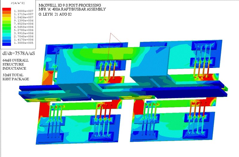
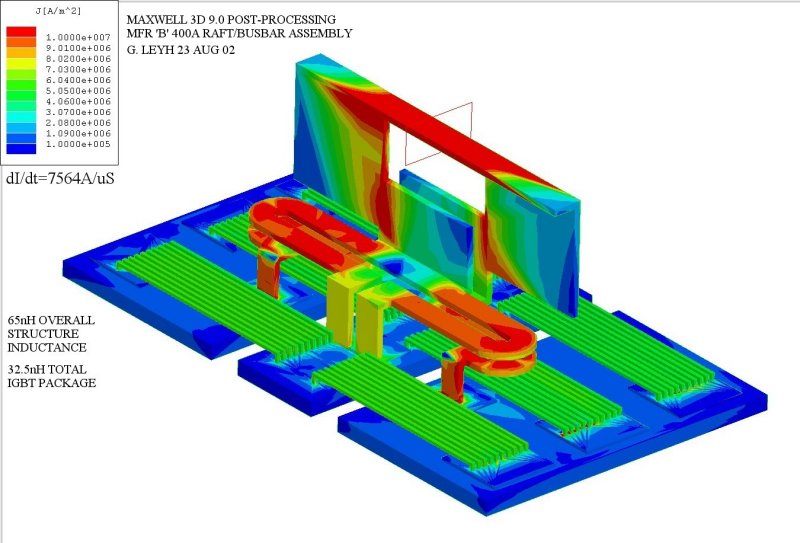
Presented here are simulation outputs showing calculated current densities on a variety of IGBT structures during fast dI/dt conditions. 3D CAD design software [SolidWorks] generated a 3D mechanical model of each system based on actual caliper measurements. The Maxwell 3D application tools assigned the desired physical material properties, boundary conditions and meshing of the structure for the simulation. The thin red rectangular window in the results below indicates where the excitation is applied to each structure. The excitation in all of the simulations is a 2000V step function, applied through an external 200nH inductor. The results also list the calculated dI/dt and the overall structure inductance, directly under the color legend. Using a voltage source with a fixed external inductor for excitation resulted in shorter simulation times than using a ramped current source. Typical computation times for these field solutions were approximately 4 hours.
|
|
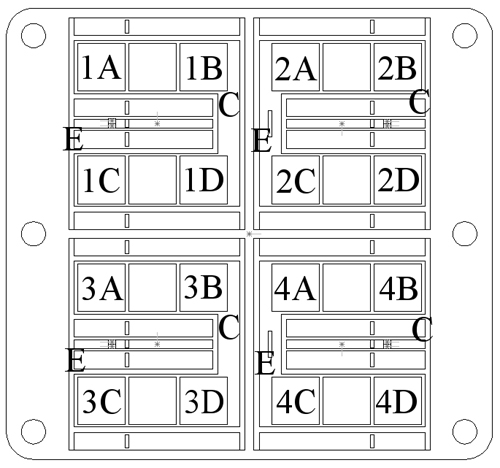
This first output represents the standard raft and busbar structure found in the 6 failed IGBTs. Note the higher current densities in locations that correspond to die locations A and C in the die position diagram [this 3D model is inverted from the diagram], and along the die edges closest to the busbar. The calculated current densities range by a more than a factor of 50 between the hottest and coldest die bonding wires.
|
|
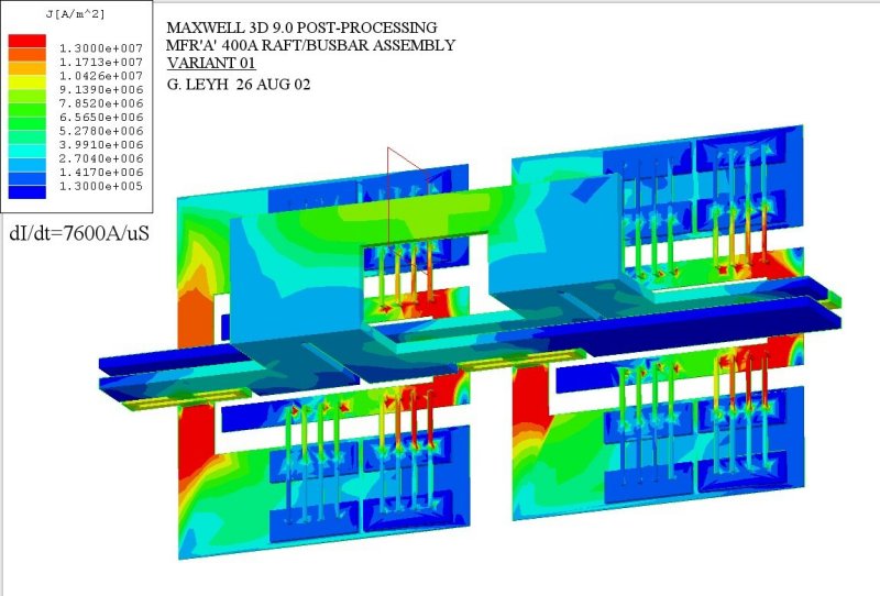
Mfr 'A' provided 5 samples of a newly configured IGBT for testing. This new configuration [Variant 01] attempts to better equalize the emitter inductances by moving the dies closer together, which is a relatively easy change from a mass-production standpoint. A simulation of this geometry indicates little difference in the current density distributions since the bonding wires are still daisy-chained across the dies.
|
|
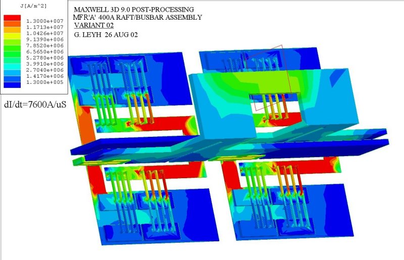
This is an alternate to the 'Variant 01' above, with the dies shifted up to the far end of the emitter trace.
|
|
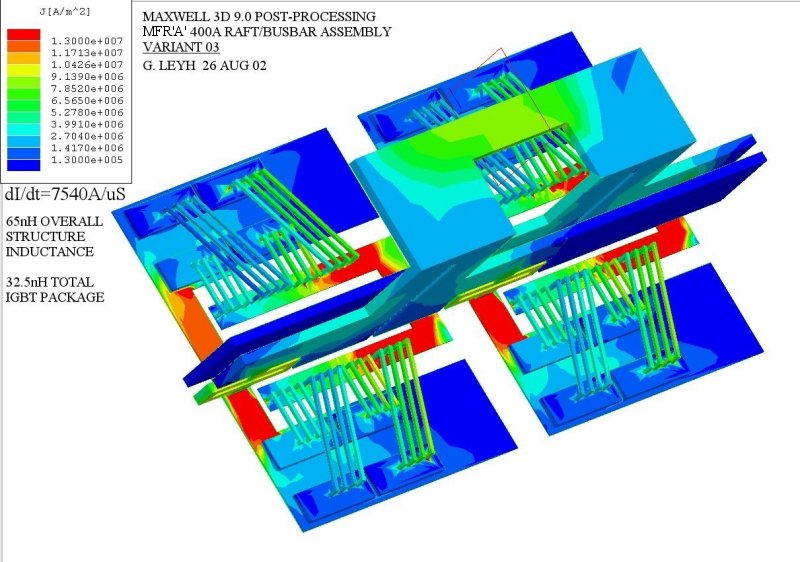
This is a hypothetical case of Variant 02 [above], where the daisy-chains are removed. Each emitter pad is given its own bonding wire, and arranged as shown to equalize the current path lengths as closely as possible. Note that the current density spread improves considerably, reduced to about 4 to 1.
|
|
Shown here for completeness is a simulation of the
Mfr ‘B’ IGBT geometry. Mfr 'B' features a radically
different busbar structure as shown below, which exhibits excellent current
uniformity under high dI/dt conditions. Unfortunately this IGBT is not suitable for the final NLC design, since it is only available up to 4.5kV [Mfr
'A' offers 6.5kV devices]. The
Mfr ‘B’ IGBT also suffers from a long turn-off tail, due to the
significantly higher hole conduction in the PT silicon technology they employ. The Mfr 'A'
silicon uses an NPT silicon technology, with significantly cleaner and faster switching performance.
This turn-off tail critically affects the switching losses. In the overall NLC design, gains in modulator efficiency of even a fraction of a percent are significant, as the total modulator grid power draw is expected to be on the order of 350 MW.
At the present time we are using IGBTs from Mfr 'B' in the modulator until we more fully understand the failure mechanisms involved with the Mfr ‘A’ IGBTs.
The simulation results above suggest several design criteria:
1] The IGBT should have a single, centrally located summation point for all of the internal emitter and collector currents instead of the standard multiple connection tabs. This prevents circuitry external to the IGBT from affecting its internal current distribution.
2] Each die raft should have an identically inductive emitter path to the internal summation point. The gate drive path should follow this emitter path closely, to minimize the coupling of fast common-mode voltages to the emitter-gate voltage.
3] Each emitter pad on each die should have independent bonding wires to the emitter trace on the raft. The bonding wires should exit symmetrically to opposite sides of the die, thus preventing one set of wires from inductively shielding the other.
4] The placement of the collector busbar should be as far from the emitter wires as practical. The geometry of the collector busbar should be symmetrical across the entire package, to minimize uneven coupling of currents back into the emitter wires.
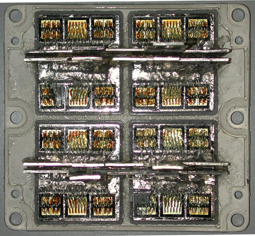
5] Each die should have its own gate resistor, to minimize cross-charging of the gates during high dI/dt and dV/dt conditions. The resistor values should be as large as practical while still allowing fast gate switching.Several IGBT packaging designs that include these concepts are considered here.