 |
ANALYSIS OF IGBT FAILURES CAUSED BY OUTPUT ARCING
During initial testing of the prototype NLC modulator in Bldg 15, an arc in the 500kV klystron output circuit damaged approximately 25% of the IGBT's in the modulator primary drive stages. A number of these failed IGBT's were removed and carefully dissected, in an attempt to determine the cause of failure.
All of the IGBTs from this prototype modulator are from one manufacturer [Mfr 'A'].
Mfr ‘A’ provides the following base specifications for these IGBTs:
Vce = 3300V
Ic continuous, 80degC = 800A
Ic 1mS pulse duration, periodic = 1600A
These megawatt class Insulated Gate Bipolar Transistors
[IGBTs] find many uses in industrial applications such as traction drives,
induction heating, paper mills and substation power factor
correction. These commercial applications place far less stringent demands on speed and
critical dI/dt performance than higher speed pulsed-power applications, such as
kicker magnets or klystron modulators -- Therefore we are operating these commercial IGBTs in mostly uncharted corners of
their IGBT parameter space. At the present time however, these IGBTs appear
to be the closest 'off-the-shelf' fit to the NLC modulator requirements, and
with some packaging and busbar modifications the Mfr 'A' product appears to be quite viable.
A single failed IGBT from another manufacturer [Mfr 'B'] was also included for evaluation here, as it might represent a practical second source for lower voltage operation.
|
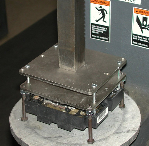
In order to minimize damage to the internal IGBT structure during disassembly, a custom fixture supports the die substrate and the busbars of the IGBT in an arbor press as shown here. The press cleanly separates the outer casing from the die substrate, leaving the internal busbar structure intact.
The manufacturer filled the interior of the IGBT with a two-part pourable silicone dielectric gel, to eliminate voids and support the die bonding wires. Removing this gel required some careful effort, to avoid damaging the dies or the bonding wires. Applying constant tension to the gel while meticulously trimming with an Exacto knife seems to yield the best results.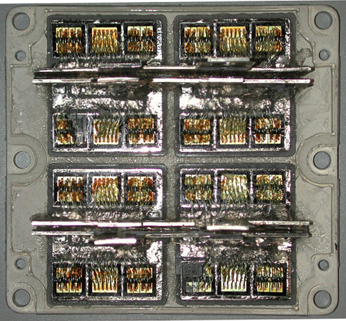 |
Shown here is an extracted IGBT die substrate from Mfr 'A', with busbars still attached and most of the dielectric gel removed. There are 16 total IGBT dies and 8 anti-parallel diodes in this package.
The failure points on the dies are readily observable. In several cases the entire die is fragmented and blown clear of the pad.
The failed die positions are summarized below for all six Mfr 'A' IGBTs.
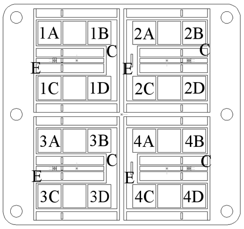 |
Positions indicated by 1A - 4D are the IGBT dies, and the 8 blank squares show the anti-parallel diode locations. The emitter and collector busbars connect to the 4 die rafts at points marked by 'E' and 'C'.
DAMAGE LOCATION SUMMARY:
1C -- 5
2C -- 4
3A -- 2
4C -- 2
One important observation -- in every case of die failure, the die failed on the side closest to the busbar.
Several patterns are readily apparent in the die failures:
1] Dies tend to fail closest to the Emitter terminal [locations A or C].
2] Dies tend to fail on the lower half of the raft [location C preferred over A].
3] Dies tend to fail in the upper half of the IGBT [Rafts 1 and 2 preferred over rafts 3 and 4].
4] Dies tend to fail along the edge of the die closest to the Emitter busbar.
Each of these tendencies has the potential for reducing the available silicon by up to 50% during a fault. The aggregate reduction from all four effects could therefore be as high as 87.5%. Such a constriction of the IGBT’s active silicon would exceed the Safe Operating Area many times over during a fault.
Measurements made on IGBTs in the test stand show that the collector current can surge as high as 7,ooo amperes as the core saturates, with a dI/dt of 1o,ooo to 2o,ooo A/uS. These fast risetimes can develop voltages on the order of 10 to 20 volts across stray circuit inductances as small as 1nH. The gate-emitter threshold voltage for these IGBTs typically lies in the range of 6 to 10 volts.
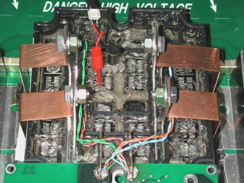 |
The custom test fixture shown here is for measuring actual dI/dt generated voltages on the the dies and buswork, using an open-faced IGBT provided for evaluation by Mfr 'A'. A miniature wide-band transformer [white cube] matches a set of micro-probes into a 50-ohm coaxial cable. The micro-probe tips have small enough features to probe the gate and emitter bonding pads directly. Locating the probe tips on the die pads during measurements requires great care, since the gel significantly refracts the apparent location on the dies, and misplacing a probe by as little as 1mm can result in a 2,ooo volt error.
The pulse duration and collector voltage were chosen to produce a dI/dt of approximately 1o,ooo A/uS. A fast CT inside the core measured the actual dI/dt. The pulse repetition rate for the test was 1Hz.
Referring to the IGBT die position diagram, the measured dI/dt induced voltages were:
| Die 2B, top left emitter pad to bottom left | 4V to 6V pk |
| Die 2B, top right emitter pad to bottom right | 4V to 6V pk |
| Die 2B, bottom right emitter pad to bottom left | 3V to 4V pk |
| Die 2B, top right emitter pad to bottom left | 8V to 10V pk |
| Emitter trace on raft 2, from 2B to 2A | 11V to 15V pk |
| Emitter busbar connection [E] to raft, from raft 1 to raft 2 | 33V to 37V pk |
| Emitter busbar connection [E] to raft, from raft 3 to raft 4 | 33V to 37V pk |
The measured voltage gradients across the die were substantial. Of primary concern were the wide variations of effective emitter-gate voltages from one area of the die to another. Due to the fast emitter currents producing large dI/dt voltage gradients across the die emitter pads, the differentially measured emitter-gate voltages on each of the 8 sections of the die ranged from 6V to 14V.
The large voltage gradients between the top and bottom halves of the die appear to be due to the 'daisy chaining' of the emitter bond wires across the die, as opposed to each pad having its own independent wire leading off the die. The voltage gradients from left to right appear to be caused by the trace inductance on the substrate.
Considering the voltage gain of the IGBTs, such a wide variation in gate drive voltage across the die would tend to divert most of the die current into a relatively small area, typically the corner closest to the raft emitter trace and furthest downstream. This would explain the tendency in all observed die failures for the dies to fail in the section closest to the emitter trace.
Given this correlation between measured voltage gradients and observed damage, the next logical step seemed to be to perform a more detailed transient EM analysis on a CAD geometry of the IGBT busbar structures. A matrix solver for EM fields by Ansoft [Maxwell 3D] performed this evaluation.